
STELA Materials Inc (SMI) (legal name is CSI2D. Inc) was founded to capitalize on new business opportunities within the semiconductor industry, particularly material science and two-dimensional (2D) substrates used for next generation manufacturing of semiconductor applications and industry applications for aerospace, computing and medical applications.
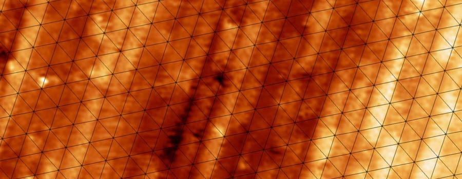
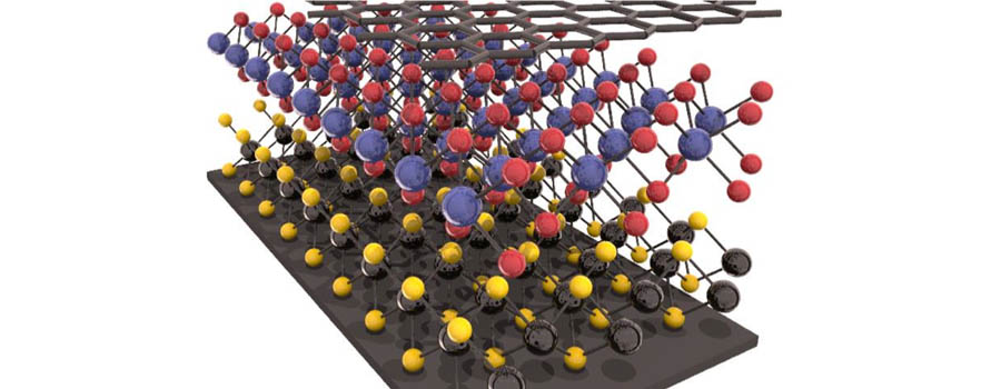
SMI has created a unique process to build two-dimensional layers of numerous materials (Graphene, Arsenene, Gallium, and Silicene) on Silicon substrates (Si 111 or Si 112 or even SiC- Silicon Carbide).
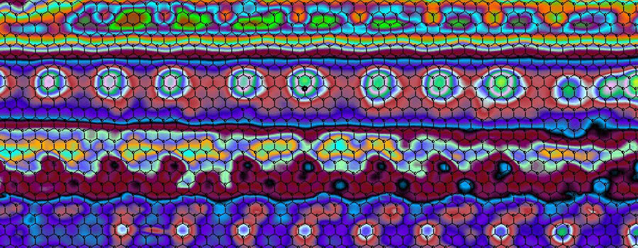
2D “layers” on semiconductor substrates has tremendous benefits for microelectronics and materials applications. The immediate benefits are a 5,000% improvement of dialectric properties- so electrons run faster, cooler, with less energy. In short- “superconductive properties at room temperature”.
To date, no other organization has been able to fabricate epitaxial 2D materials onto silicon substrates fast, cost-effectively, stable, and with a high-degree of repeatability (e.g. minimal waste). Since silicon is the base substrate for almost every electronic device, our process enables a simple way to increase the performance of many applications in many markets.
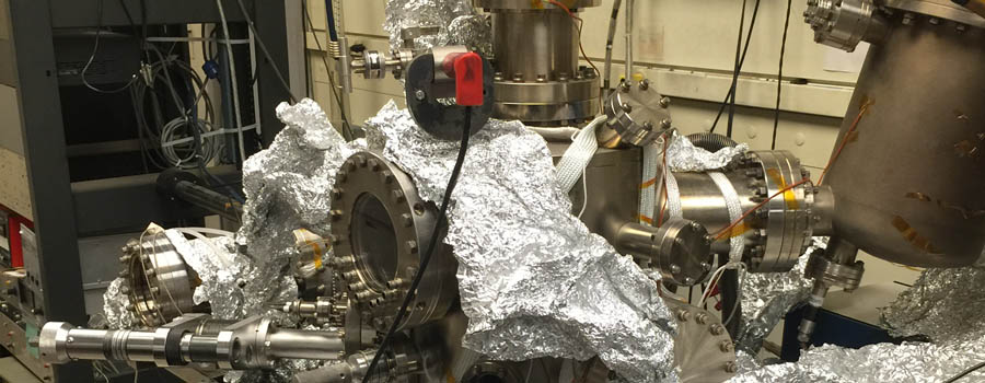
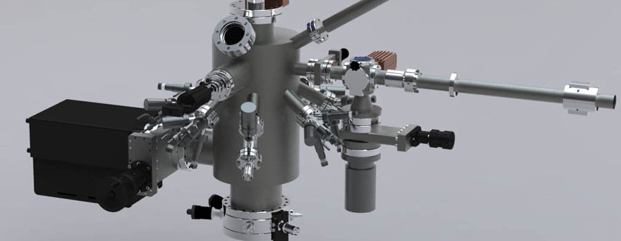
Technology
The world’s first 2D substrates on silicon are enabling a new era in semiconductors with significant increases in manufacturing speed, precision and affordability.
These will be seen to catalyze device development for a wide range of next generation semiconductor implementations. 2D layers on silicon substrates represent a major evolutionary and developmental leap on the path to dramatically more efficient devices built on superior substrates. These materials enable the following features:
- CPU/ GPU's- 100x computational throughput and faster read-write cycles
- 50x memory density improvements where none were thought to be possible
- photovoltaics energy density improvements- superior transparency enables light to produce electricity within the actual semiconductor chip- 50 to 75% efficiency is expected with both visible and UV light
- Electric motor/generators operating at 10kV with 100x power over current form factors
- Batteries supporting 50x current watt/hr/kg densities
Presently SMI can produce Graphene on Silicon Carbide, amongst many other materials as outlined above (Learn more here). Our list of world-leading technical advancements is growing everyday. We have made various substrates on Silicon that are "world first's" (as of December 2016):
- Arsenene on Silicon
- Silicene on Silicon
- Graphene on Silicon Carbide on Silicon
- Graphene encapsulated TaC on Silicon Carbide on Silicon
Our wafers are the best, most scalable in the world, exceeding other manufacturer’s specifications. SMI's innovative, scalable production technique improves quality, reduces time and reduces cost for manufacturing semiconductors. The immediate benefits are substantial improvements in circuit density, power efficiency and performance for various devices. BUY samples of our wafers here for research and testing purposes.
Market Opportunities
SMI 2D substrates enable next-generation applications for any number of markets/ applications- all are multi-billion dollar markets. The following verticals have the most immediate needs:
- Power (solar cells, batteries, fuel cells, grid, etc)
- Network/ Computing (memory, storage, CPU, quantum, network)
- Health (bio-compatibility, bio-mechanical)
- Telecommunications (fiber optics, switching)
- Defense/ Security (imaging sensors, biology-nuclear sensing)