How & Why:
There is strong effect of low energy ion bombardment on the material surface; it changes with surface Debye temperature.
The Debye temperature is lower for higher doses of ion bombardment. Notably, the greater ion doses correlate with defects on the Si(111) surface.
SMI’s experiments lead to the conclusion that the Debye-LEED method for analysis will be useful for effective defect characterization and epitaxial materials synthesis for the following processes:
- semiconductor wafers
- hetero-structure epitaxial growth
- 2D materials
The Debye-LEED method helped SMI to synthesize the epitaxial hexagonal TaC on SiC(0001)-4H with graphene encapsulation by measuring “strange” variations in surface Debye temperature with electron beam energy.
Potential application of this method are significant! For starters, it enabled SMI to grow epitaxial II-VI materials with graphene encapsulation (a world first!)!
Debye-LEED instrumentation is relatively simple and flexible in the adaptation to both MBE systems or other deposition and wafer processing machines; especially at the wafer surface preparation stage.
Characterizing Defects in Semiconductors
It’s vital to characterize semiconductor surface defects as it permits one to reduce & control them. Defects are enormously costly, and wasteful, in the manufacturing of semiconductors.
“Defects science” in semiconductor materials is complex because of the different nature of defects that result from:
- The wafer manufacturing processes;
- The chip fabrication process; and
- Metal or gas contamination.
It’s critical to characterize the defects at the beginning of wafer substrate stage preparation. There are about 200 stages in the chip fabrication process on silicon wafers. It takes about 6-8 weeks to complete the process; so reducing (or eliminating) defects at the beginning of this process is less costly (in terms of expense and time-to-market).
The primary source of defects formation on semiconductor wafers is the growth of the “hetero-structures” that result from “lattice mismatch”.
2D materials offer unique properties for new semiconductor fabrication methods. That means, there is an opportunity to produce better, faster, cheaper materials and devices for photovoltaic, battery and clean energy electrochemical systems.
The defects in low-dimensional crystals in 2D materials are critical for their functionality. Conventional microscopy techniques have very limited application.
There are a large number of defects characterization techniques:
- Preferential etching combined with optical microscopy and scanning electron microscopy
- Transmission electron microscopy
- X-ray topography and diffraction
- Scanning Probe Microscopy
- STM- scanning tunneling microscopy
- AFM- atomic force microscopy
Surface Debye Temperature Methodologies
Surface Debye temperature measurements are based on the Debye thermodynamic model of atoms vibrating with changing frequency related to the temperature of the crystal.
The thermal vibration of the atoms in the crystal depends on the atomic bonding, lattice parameters, surface energy and also defects.
Up to now, there has been no link between the thermal vibrations characteristic of the atoms, such as Debye temperature, and the defects concentration.
When you look on the crystal atomic lattice, it seems obvious that such link must be present. When you take a one dimensional chain of atoms and examine their “vacancies”, the thermal vibrations will be different because there are empty spaces with broken atomic bonds. Such a defect will be reflected in the thermal vibration of the atoms and, as a result, it will have lower Debye temperature.
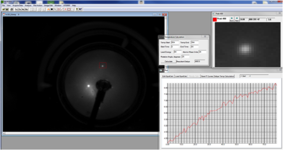
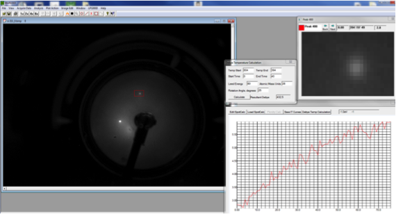
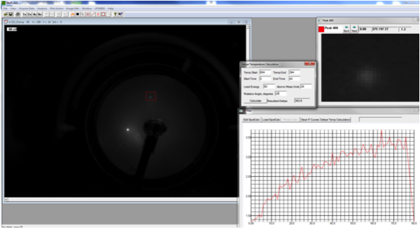
The motivation for SMI's team of researchers was to prove the relation between defects and effective Debye temperature. Surface Debye temperature can be measured using low energy electron diffraction (LEED). LEED is a very well-established technique for surface crystallography. LEED has been used for the surface defects characterization using the spot profile analysis of the "diffraction spot".
Debye- LEED
In the past, LEED was used to measure the effective Debye temperature. These measurements are based on the "diffraction spot" intensity changes due to thermal vibration of the atoms. The intensity is lower for higher temperatures because the atoms vibrates with higher frequency and reduce surface ordering.
From the intensity changes vs. temperature changes, the effective Debye temperature can be calculated.
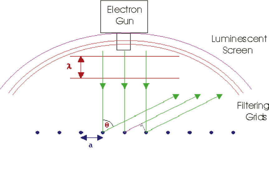
LEED
LEED is an established technique for surface structure of ordered crystals, disordered arrays and over-layers. LEED formalism includes:
- pattern analysis
- I-V analysis
- spot-profile analysis for defects
- Debye-LEED measurements
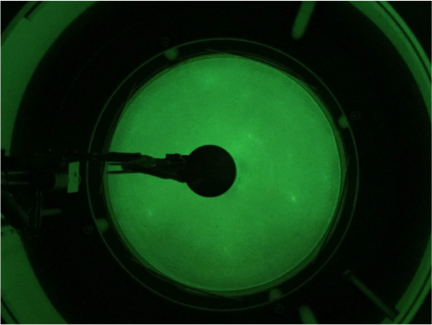
 LEED Spectrometer
Two factors are critical: suitable wavelength and limited penetration depth. These factors determined LEED as a potential probe for surface geometrical structures
SPA- LEED
There are limitations of the defects characterization by Spot Profile LEED
This method is measuring only defects associated with the coherence length and coherence area of the sample for the ordered structure. The disorder structure contributes only to the LEED pattern background increase.
The surface Debye temperature reflects contribution from all defects at the surface and below for higher energy beam as the effective parameter is sensitive to the defects concentration.
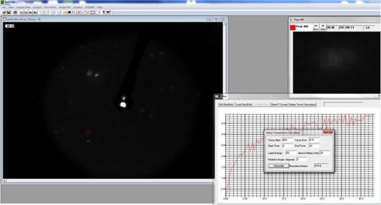
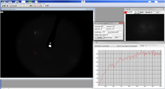
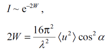
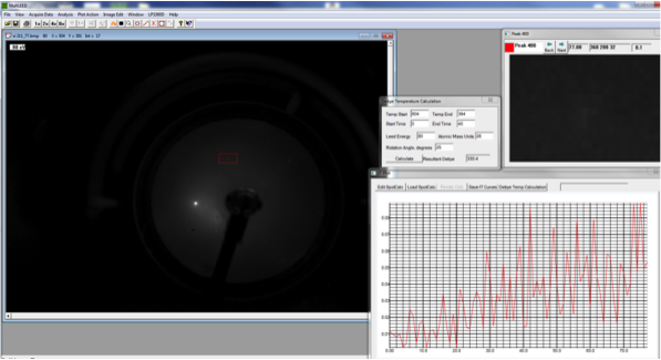
Debye-LEED Calculation
|
The intensity “I” of a diffracted electron beam decays exponentially with increasing temperature due to the increase in the thermal vibration. Surface Debye temperature is calculated from the measurements of the intensity change as a function of sample temperature. |
|
| “N” is Avogadro’s number, “ħ” is Planck’s constant divided by 2π, “T” is the temperature of the sample (in Kelvin), “k” is the Boltzmann constant, “M” is the molar mass of vibrating atoms of the lattice and “Θ” is the characteristic Debye temperature of the lattice. | 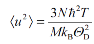 |
Effects of Low energy Argon Ion bombardment
Ion Sputter Gun- model IG70-X-Y ( OCI)
Purity of Ar gas: 99.998 %
Argon beam energy: 500 eV
Ion Beam Current: 0.5 uA
Ar+ doses: 10exp12/cm2 of ions (0.001 of monolayer coverage)
Bombardment Angle: Normal to the surface
Ion Beam Size: 10 mm diam.
Sample temperature during ion bombardment
System geometry: Si(111) sample was rotated form LEED optics to the ion sputter gun
STM photos:
|
STM from Si(111) before ion bombardment |
STM from Si(111) after ion bombardment |
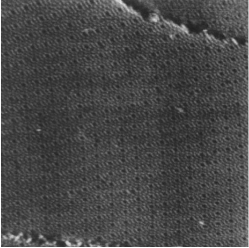
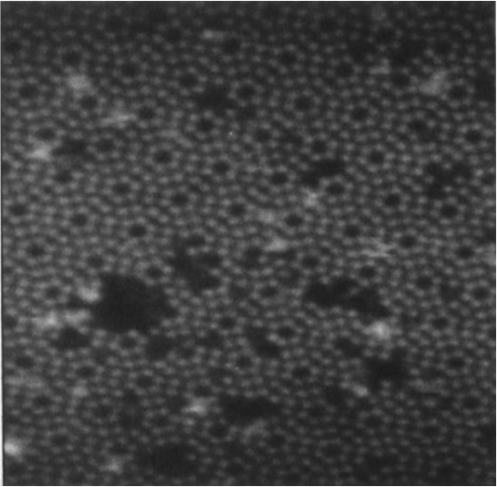
Ion bombardment creates atom “vacancies” with depth of monoatomic steps. Annealing of the bombarded surface at 750 C produces complete restoration of the 7x7 structure
 Debye-LEED on Si(111) under Ar+ 500eV
Si(111) 7x7 wafer is good system model:
- well studied surface
- it is thermodynamically stable
- atom concentration 16 x 10 exp14 atoms per cm2
- lowest surface energy ( 0.9 eV per Angstrom)
- because Si-Si bonds are directed along <111> direction
- Ar+ sputtering rate: 0.4 atoms per ion
- Vacancy creation rate: 10-20 vacancy per Ar+ ion
Debye-LEED Data for Si(111) under Ar+ 500eV
 |
 |
 |
 |
|
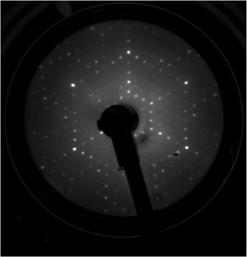
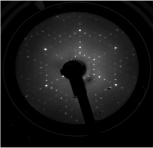
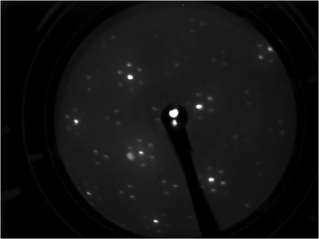
LEED pattern form Si(111) 7x7 |
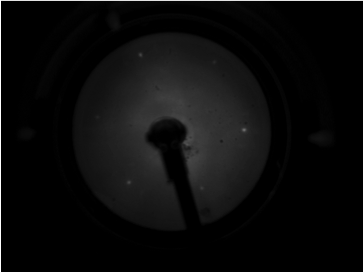
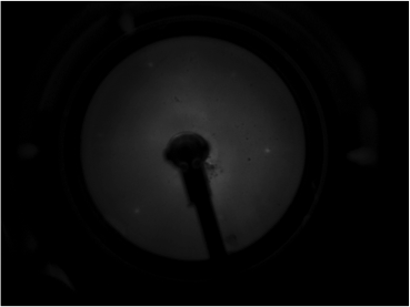
LEED pattern form Si(111) 1x1 |
LEED pattern form Si(111) 1x1 |
How to do Synthesis of hexagonal TaC on 4H-SiC(0001)?
2D materials, such as graphene, offer very unique properties that can be utilized in semiconductor device fabrication and SiC(0001) is good for growing epitaxial graphene.
Ref. Recent paper: “Two-dimensional GaN realized via graphene encapsulation” – Z. Al. Balushi at all., Nature Materials, Published on line August 26, 2016. Substrate was 6H-SiC(001)
- TaC is a good material to grow on SiC because of the low lattice mismatch
- TaC presents a strong chemical reaction to SiC, even at temperature as low as 400C
- The combination of these two factors was the impetus to make TaC synthesis on SiC(0001) with the graphene layer
- The synthesis was done with annealing the TaC plate contacting the SiC wafer.
- For the first step- a disordered TaC layer is formed (see photo below)

STELA Materials used our MBE 1300 system
- Debye-LEED/AES, model BDL800IR-MCP1
- Ion sputtering gun, model IG70-XY for surface cleaning, low energy
- 7 deposition sources with water and LN2 cooling
- Thin Film quartz crystal thickness monitor
- X-Y-Z-R manipulator with 1600 C sample heating stage
- Sample transfer, load lock and sample storage for 6 samples
- Mounting flanges for integrated XPS/UPS in the same chamber
- Mounting flanges for RHEED in the same chamber
- Ion pump, TSP pump with LN2 cooling and turbo pump
- Bakeout tent and timers
- Compatible with UHV sample transfer to RHK STM microscope
STELA's Children ->> Graphene on hexagonal TaC on 4H-SiC(0001)
|
LEED pattern form- disordered |
LEED pattern form- ordered Graphene on hexagonal TaC on 4H-SiC(0001), |
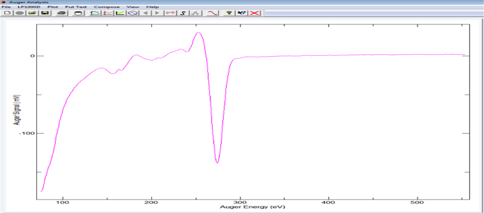
AES spectrum from Graphene on TaC on 4H-SiC(0001)
|
|
Debye-LEED from Graphene on TaC on 4H-SiC(0001) |
Debye-LEED from Graphene on TaC on 4H-SiC(0001) |