
Experimentation was conducted from 2013 to 2015 to identify a stable and affordable process to form or deposit Silicene and Arsenene on a variety of Silicon surfaces. SMI's early experiments focused on fabricating an Arsenene layer on Silicon (112) as a baseline to prove process efficacy for additional substrate materials, with a focus on Silicon (112) substrates as the most compelling outcome for major advancements in semiconductor manufacturing for lattice matching.
Tests were conducted to verify the silicene/arsenic substrate interfaces had exhibited uniform dimensional features, and to establish that purity of silicene deposition was not corrupted by oxygen at the interface. Evidence was first recorded using an STM, LEED, XPS, and other analytical techniques.
Monolayer Arsenic use for improved lattice matching in (II-IV) detectors was then tested and found to form an Arsenene surface layer. Using a proprietary ultra-high vacuum annealing reactor and MBE (see "Stela" above), SMI's principal scientist conducted a series of trials under varying temperature and annealing times to optimize the surface layers' uniformity for Arsenic covered clean silicon surfaces. Tests were conducted to verify the silicene/arsenic substrate interfaces had exhibited uniform dimensional features, and to establish the purity of silicene deposition was not corrupted by oxygen at the interface.
Evidence was first recorded using an STM, LEED, XPS, and other analytical techniques, which is summarized in the following exhibits:
|
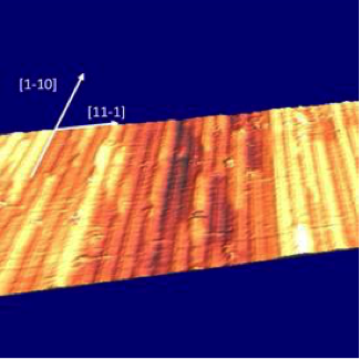
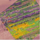
The structures on the surface are periodic, with 2 nm rows running in the [1-10] direction. |
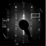
LEED images of the arsenene covered clean Si(112) have been matched to a very large unit cell, similar to that of a silicene monolayer on Si(112). |
|
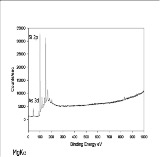
XPS studies show no other atoms than silicon for the clean anneal studies and silicon and arsenic for the MBE of the arsenic monolayer studies. |
Two STM images of separate surfaces, one of the clean, aggressively annealed Si(112) surface, and one of the monolayer of arsenic MBE deposited during annealing on the clean annealed Si(112) surface, show the same large surface structure topology over a 50x50 nm region. |
Validation
The SMI team makes various 2D materials and had top industry nano-materials specialists/ leaders validate that SMI can reproduce 2D materials on various substrates. In short, industry experts have proven that SMI can easily fabricate silicene, graphene, arsenene on Si 111, Si 112 and SiC.
The properties of those materials are interesting. The graphene dialectric properties show that electrons move at the speed of light with no heat and no resistance- in short, "superconductivity at room temperature". SMI can reproduce this material all day long and numerous tests with LEED, STM, SEM show the material is consistent.
No current indicators suggest that an efficient Silicene or Arsenene production process has been perfected by other entities; but significant levels of academic and corporate research efforts are focused on possible solutions.